School on Nanotech
updated to September 11th, 2020
|
September 16-17-18 |
||||||||||
|
The School will be held REMOTELY |
||||||||||
| Chairs: Lorenza FERRARIO, FBK & Vittorio MORANDI, CNR-IMM | ||||||||||
| Co-organized with | ||||||||||
 |
||||||||||
|
The course is dedicated to Master degree and Ph.D students, as well as to scientists working in the wide field of micro- and nano-technology, offering the opportunity to learn about sensors and actuator fabrication and characterization processes, with attention to both planar and 3D technologies. Besides the lectures dedicated to single technology steps, building blocks of the silicon-based micro- and nano-fabrication technologies, there will be sessions dedicated to devices application areas, like sensors for Quantum Technologies, piezo actuators and other. The workshop will be completed with a live lesson from the FBK cleanroom CR D, to practically show some of the fundamental silicon processing steps. The school is organized by It-fab (http://itfab.bo.imm.cnr.it/), the Italian network for Micro and Nano Fabrication research infrastructures, in collaboration with STMicroelectronics Italy. The School will be held REMOTELY |
||||||||||
| ROOM 10 | ||||||||||
| Wednesday 16 September | ||||||||||
| 14:00 - 14:05 | Welcome and Introduction Vittorio MORANDI - CV, CNR-IMM, Bologna |
 |
||||||||
| 14:05 - 14:20 |
Introduction to micro- and nano-fabrication Lorenza FERRARIO, FBK |
 |
||||||||
| 14:20 - 15:05 |
Deposition techniques Riccardo BERTACCO, PoliFAB |
 |
||||||||
| 15:05 - 15:50 |
Litography Stefano SORESI, Inphotec |
 |
||||||||
| 15:50 - 16:35 | Etching Fulvio MANCARELLA, CNR-IMM, Bologna |
 |
||||||||
| 16:35 - 17:20 | Direct Laser Writing Sara NOCENTINI, INRIM |
 |
||||||||
| ROOM 10 | ||||||||||
| Thursday 17 September | ||||||||||
| 11:00 - 11:45 | 3D printing and two photon polymerization: toward the rapid prototyping of micro- nano- devices Valentina BERTANA, Chilab & Polytechnic of Turin |
 |
||||||||
| 11.45 - 12:30 | Micro- Nano- devices for bio: How to develop a Lab on a chip and a biosensor Simone Luigi MARASSO, Chilab & Polytechnic of Turin |
 |
||||||||
| Break time | ||||||||||
| 14:30 - 15:15 | Photonics packaging: laser hybrid integration towards space applications Aina SERRANO RODRIGO, Inphotec |
 |
||||||||
| 15:15 - 16:00 | High-density W-filled TSVs for advanced 3D-Integration Josef WEBER, FHG |
 |
||||||||
| 16:00 - 16:45 | System level 3D integration and system-in-package for chemical sensing microsystems Stefano ZAMPOLLI, CNR-IMM, Bologna |
 |
||||||||
| 16:45 - 17:30 | Metrological approach to 3D SERS platform characterisation Eleonora CARA, INRIM |
 |
||||||||
| ROOM 10 | ||||||||||
| Friday 18 September | ||||||||||
| 10:00 - 10:30 |
Ion-induced nanopatterning of semiconductor surfaces: a short link between basic research and applications |
 |
||||||||
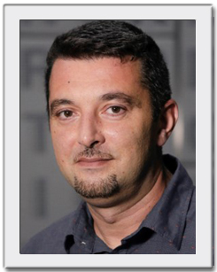
| 10:30 - 11:00 | QT/photonics devices; FET project with 3D integration for QT Mher GHULINYAN, FBK |
 |
||||||||
| 11:00 - 11:30 | Materials, Sensors and Actuators in MEMS technology evolution Andrea PICCO, STMicroelectronics |
 |
||||||||
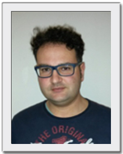
| 11:30 - 12:00 | UV Sensor Technology Integrated on Unmanned Aerial Vehicle for Air Pollution Monitoring Massimo CUSCUNA' e Marco CASELLA, CNR Lecce |
 |
 |
|||||||
| 12:00 - 12:30 |
Superconducting Metamaterials for Microwave Photonics at the Single Photon Level |
 |
||||||||
| 12:30 - 13:00 |
Flexible and large area electronics |
 |
||||||||
The School will send a certificate of participation with the programme and the total number of lessons hours. The document will be sent to registered people only and has to be requested explicitly to This email address is being protected from spambots. You need JavaScript enabled to view it.

