SPM School
| School on Scanning Probe Microscopy September 16-17-18 |
The NanoInnovation 2020 SPM School is mainly intended for graduate and PhD students as well as young scientists interested in deepening their knowledge about advanced SPM methods, but it is also open to all researchers and scientists who are involved in the different fields characterizations methods for nanotechnology and nanosciences.
As for all the NanoInnovation events, the attendance to the NanoInnovation 2020 SPM School is free and the interested attendees are requested to register using the NanoInnovation website selecting the option “SPM School” in the online form.
 |
 |
| ROOM 6 | ||||
|
|
||||
| I. Nanomechanical mapping Chair: Daniele PASSERI - CV |
||||
| 10:45 - 11:00 |
Welcome and Introduction |
 |
||
| 11:00 - 11:45 | Nanomechanical mapping of soft materials with the atomic force microscope: methods, theory and applications Ricardo GARCIA - CV, CSIC |
 |
||
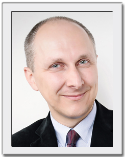
| 11:45 - 12:30 | The utilization of fast AFM’s tip-sample interaction for the surface morphology imaging and mechanical properties mapping Andrzej SIKORA - CV, Wroclaw University of Science and Technology |
 |
||
| Break time | ||||
| II. Electric and thermal phenomena in 2D materials Chair: Andrzej SIKORA - CV |
||||
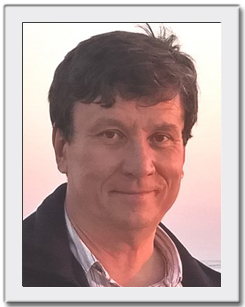
| 14:00 - 14:45 | Exploration of nanoscale thermal transport and thermoelectric phenomena in 2D materials via scanning probes Oleg KOLOSOV - CV, Lancaster University |
 |
||
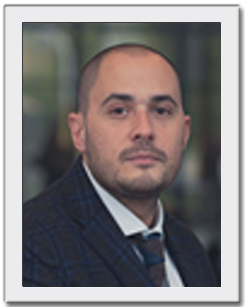
| 14:45 - 15:30 | Electrical SPM for 2D materials Umberto CELANO - CV, IMEC |
 |
||
| Break time |
||||
| III. From atoms to molecules Chair: Francesco MARINELLO |
||||
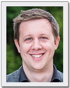
| 16:00 - 16:45 | Atomically Precise Molecular Design: Insights From Sub-molecular Resolution Scanning Probe Microscopy Samuel JARVIS - CV, Lancaster University |
 |
||
| 16:45 - 17:30 | Self-organization of complete organic monolayers via sequential post-deposition annealing: an investigation by Scanning Probe Microscopy Cristiano ALBONETTI - CV, CNR |
 |
||
| ROOM 6 | ||||
|
|
||||
| IV. Toward tomography Chair: Andrzej SIKORA - CV |
||||
| 11:00 - 11:45 |
3D tomographic AFM using Scalpel SPM |
 |
||
| 11:45 - 12:30 | Nanoscale 3D imaging of physical properties of materials Oleg KOLOSOV - CV, Lancaster University |
 |
||
| Break time |
||||
| V. Pre- and post-eperiment issues Chair: Daniele PASSERI - CV |
||||
| 14:00 - 14:45 | Correlative microscopy – the issue of precise positioning of the sample and its impact on the experiment outcome Andrzej SIKORA - CV, Wroclaw University of Science and Technology |
 |
||
| 14:45 - 15:30 | Data processing in SPM Francesco MARINELLO - CV, University of Padua |
 |
||
| Break time |
||||
| VI. Nanomagnetic characterizations Chair: Umberto CELANO - CV |
||||
| 16:00 - 16:45 | Characterization of nanomagnets by Advanced Magnetic Force Microcopy Agustina ASENJO - CV, CSIC |
 |
||
| 16:45 - 17:30 | Direct and Indirect Magnetic Force Microscopy in Histology Gunjan AGARWAL - CV, The Ohio State University |
 |
||
| ROOM 6 | ||||
|
|
||||
| VII. Nanoelectric characterizations Chair: Francesco MARINELLO |
||||
| 11:00 - 11.45 |
Carrier profiling with SPM application in Nanoelectronics |
 |
||
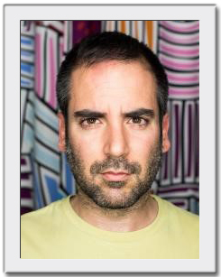
| 11:45 - 12:30 | Electrical nano-characterization of wide band gap semiconductors (silicon carbide) devices by scanning probe microscopy Patrick FIORENZA - CV, CNR |
 |
||
| Break time |
||||
| VIII.Tunneling and spectroscopies Chair: Umberto CELANO - CV |
||||
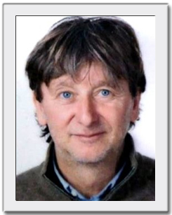
| 14:00 - 14:45 |
Basic principles of STM/S and applications to condensed matter physics |
 |
||
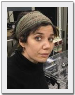
| 14:45 - 15:30 |
AFM-assisted infrared nanospectroscopy |
 |
||
| Break time |
||||
| IX. Multiferroics Chair: Daniele PASSERI - CV |
||||
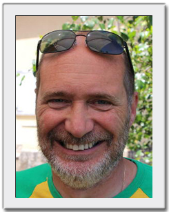
| 16:00 - 16:45 | Ferromagnetic, ferroelectric and multiferroic nanostructures. AFM characterisation Bernard NYSTEN - CV, UCLouvain |
 |
||
| 16:45 - 17:30 | SPM techniques for ferroelectric materials characterization Francisco FLORES RUIZ - CV, Benemérita Universidad Autónoma de Puebla |
 |
||

